Introduction
Transistors, which are tiny electronic components, have two main uses. They can act as switches to control circuits and amplify signals. There is a rating for a particular voltage and current for each transistor. The three pins on modern transistors typically represent the emitter, base, and collector, respectively, of the transistor. The emitter, base, and collector are represented by these letters. Transistors of the anybody type on the left have a flat edge. The NPN and the PNP are the two primary types of bipolar transistors.
Transistor
Small electronic parts called transistors serve two main purposes. They can amplify signals and serve as switches to control circuits. The metal body transistors are typically found mounted on a heat sink, which helps to dissipate the extra heat. However, we can just use these resin body transistors, which don’t need a heat sink, for electronic circuits with low currents.
There is writing on the transistor’s body. We can use the part number provided by this to locate the manufacturer’s datasheet. It is crucial to review these sheets because each transistor has a rating for a specific voltage and current. The transistors now have three pins is typically the emitter, the middle is the base, and the right side is the collector in these resin with the labels E, B, and C. These letters stand for the emitter, base, and collector. The left anybody type transistors with a flat edge. However, not all transistors operate in this manner.
We are aware that a light bulb will illuminate when connected to a battery. By adding a switch to the circuit, we can control the light by cutting off the power. We make use of a transistor for that. The current flow is obstructed by this transistor. The light is thus off. However, the transistor starts allowing current to flow in the main circuit if we apply a tiny voltage to the base pane in the middle.
The light then comes on. Then, we can attach a switch to the controlling pin to enable remote control of the device. For the transistor to turn on, we typically need to apply at least 0.6V to 0.7V to the base pin. On the main circuit, a small change in the base pin’s voltage has a big impact. Therefore, the transistor functions as an amplifier when a signal is applied to the base pin.
A very simple amplifier could be created by connecting a microphone that changes the voltage signal on the base pin to the main circuit. The base pin typically has very little current flowing through it. Much more current flows through the collector. The current gain is the ratio between these two.
What is a junction?
A junction is any location in a circuit where a current can split. Junctions differ from nodes in that they are points. In contrast to nodes, which are both the points of connection and their connecting wires, junctions do not include the wires of equal voltage surrounding them. When several conductors or semiconductors come into physical contact, the result is an electrical junction. Thermoelectricity junctions, metal-semiconductor junctions, and p-n junctions are a few different types of electrical junctions.
NPN Transistor
The NPN transistor is one of the widely used bipolar junction transistors. Essentially, it consists of two n-type semiconductors fused together. It has three terminals which are the emitter, base, and collector. Out of these three terminals, the doping concentration of the collector is the most, the emitter is moderately doped and the base is lightly doped and thin compared to the other two terminals. The NPN transistor can be also considered as two back-to-back PN junction diodes formed by the emitter-base and the collector-base junctions. In this type of transistor, the electrons act as the majority charge carriers.
PNP Transistor
The PNP Transistor consists of three semiconductor layers, where two are p-type and one is n-type. The n-type semiconductor is sandwiched between the two p-type semiconductor layers. The two p-type regions form the emitter and collector terminals and are doped more heavily than the n-type region which forms the base. Here, the electrons from the minority charge carriers and the holes are the majority charge carriers. In the case of a PNP transistor, the polarities are reverse of that of an NPN transistor, so here the current ‘sinks’ into the base, whereas in the case of an NPN transistor, the current is ‘sourced’ from the base.
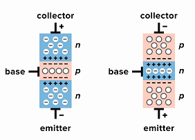
Fig:1 NPN and PNP transistors
Applications of the Junction Transistor
Logic circuits use the bipolar junction transistor (BJT).
The BJT is used as:-
- Oscillator.
- Amplifier.
- Multivibrator
- Clipping circuits for wave shaping.
- Demodulator
- Modulator.
- Implemented in time delay circuits.
Conclusion
There are two primary uses for transistors, which are tiny electronic components. They can amplify signals and function as switches to manage circuits. Each transistor has a rating for a specific voltage and current. Modern transistors typically have three pins which stand for the transistor’s emitter, base, and collector, respectively. These letters stand for the emitter, base, and collector. The anybody type of transistor on the left has a flat edge. The two main types of bipolar transistors are NPN and PNP. In this article, we have learned about junction transistor, junction of a transistor, NPN transistor, PNP transistor, Applications of junction transistor, and some FAQs.
FAQs
Q1. Why is a bipolar junction transistor called that?
Ans: The bipolar junction transistor operates by causing negatively charged electrons and their positively charged counterparts (the holes in the crystal lattice representing an absence of electrons) to exist briefly in each other’s presence.
Q2. Who created the BJT?
Ans: Bipolar junction transistors (BJTs) made of germanium alloy were created in 1948 by Bardeen, Brattain, and Shockley, and they completely changed the electronics sector.
Q3. Is a voltage-controlled BJT device present?
Ans: A physicist might claim that the basic function of a BJT is to narrow the depletion zone by applying an electric field across the base-emitter junction. This electric field, which is expressed in volts, governs how charge carriers move. Hence, the BJT is voltage controlled.
Q4. Why is a minority carrier device called a BJT?
Ans: The injected electrons or holes from the emitter are minority charge carriers from the perspective of the base. The reverse biased Collector Base Junction allows the conduction in the transistor by sweeping these minority carriers across it.
Q5. What does the BJT concentration gradient mean?
Ans: Within the base, the gradient of minority charge carriers’ concentration is elevated. Emitter-current increases with increasing reverse collector voltage since the hole current injected across the emitter junction is proportional to the minority carrier gradient.
Q6. Which BJT terminal has a high doping level?
Ans: Emitter Heavy doping is used on the emitter in order to inject a large number of charge carriers into the base. The base, which is extremely thin and lightly doped, transmits the majority of the charge carriers injected by the emitter to the collector.